

sm:leading-[6px] sm:text-sm”>
You may like
-
Rapidus to reportedly install 10 EUV chipmaking tools at its fab in Japan
-
ASML teams up with Imec for sub-2nm process technologies with High-NA EUV chipmaking tools
By now, Intel has made significant strides in developing production ready photomasks, resists, OCP, and other elements of High-NA EUV production flow. However, it looks like the obstacles associated with adoption of High-NA EUV tools by the industry are not only engineering challenges, but also economic hurdles associated both with infrastructure development and usage scenarios.
Not yet ready for prime time
One of the challenges with High-NA EUV lithography is the two times smaller exposure field compared to Low-NA EUV lithography due to higher numerical aperture of projection optics: 26 mm × 16.5 mm vs. 26 mm × 33 mm.
This is a major challenge for large chips like GPUs and CPUs, which often exceed the 13×26 mm limit of a single High-NA exposure. Therefore, to pattern these dies, two or more overlapping exposures (stitched fields) must be used (an alternative is to use a multi-chiplet designs). This introduces alignment complexity, risks of overlay errors, and yield loss in the stitched regions. Also, with fewer chips fit per exposure field, more passes per wafer are required, which reduces the wafer-per-hour rate and increases cost per wafer.
ASML proposes to use accelerated stages (i.e., accelerate how the wafer moves under the photomask) to compensate for higher number of exposures. However, Intel has long proposed to use a larger 6×12-inch photomask instead of industry-standard 6×6-inch photomask. A larger photomask solves the half-field problem by doubling the reticle area, allowing it to hold two adjacent half-field images side by side. When used with appropriately configured High-NA optics, this enables the system to expose a full 26 mm × 33 mm field in one scan pass, restoring the field size to that of Low-NA tools. This obviously eliminates the need for stitching and all the challenges associated with it.
However, the shift to larger photomasks would require a complete overhaul of the mask supply chain, from blank preparation and e-beam writing to handling and fab integration. ASML acknowledged that internal studies on larger masks are in progress but has not committed to bringing the capability to market. The change would disrupt the company’s platform unification strategy for Low-NA, High-NA, and eventually Hyper-NA tools and potentially reduce sales of higher-end tools.
In photoresist development, metal-oxide resists are gaining ground as the preferred option for High-NA, according to the Intel’s presentation at SPIE. These materials provide better performance in terms of resolution, line-edge roughness, and dose sensitivity, especially important given the thinner films required by the thin depth-of-focus associated with High-NA optics. Traditional chemically amplified resists struggle with etch resistance at the thicknesses now needed, while metal-oxide formulations retain sufficient durability during pattern transfer. Most SPIE 2025 data shared for High-NA tools used metal-oxide resists rather than legacy organics, according to SemiAnalysis.
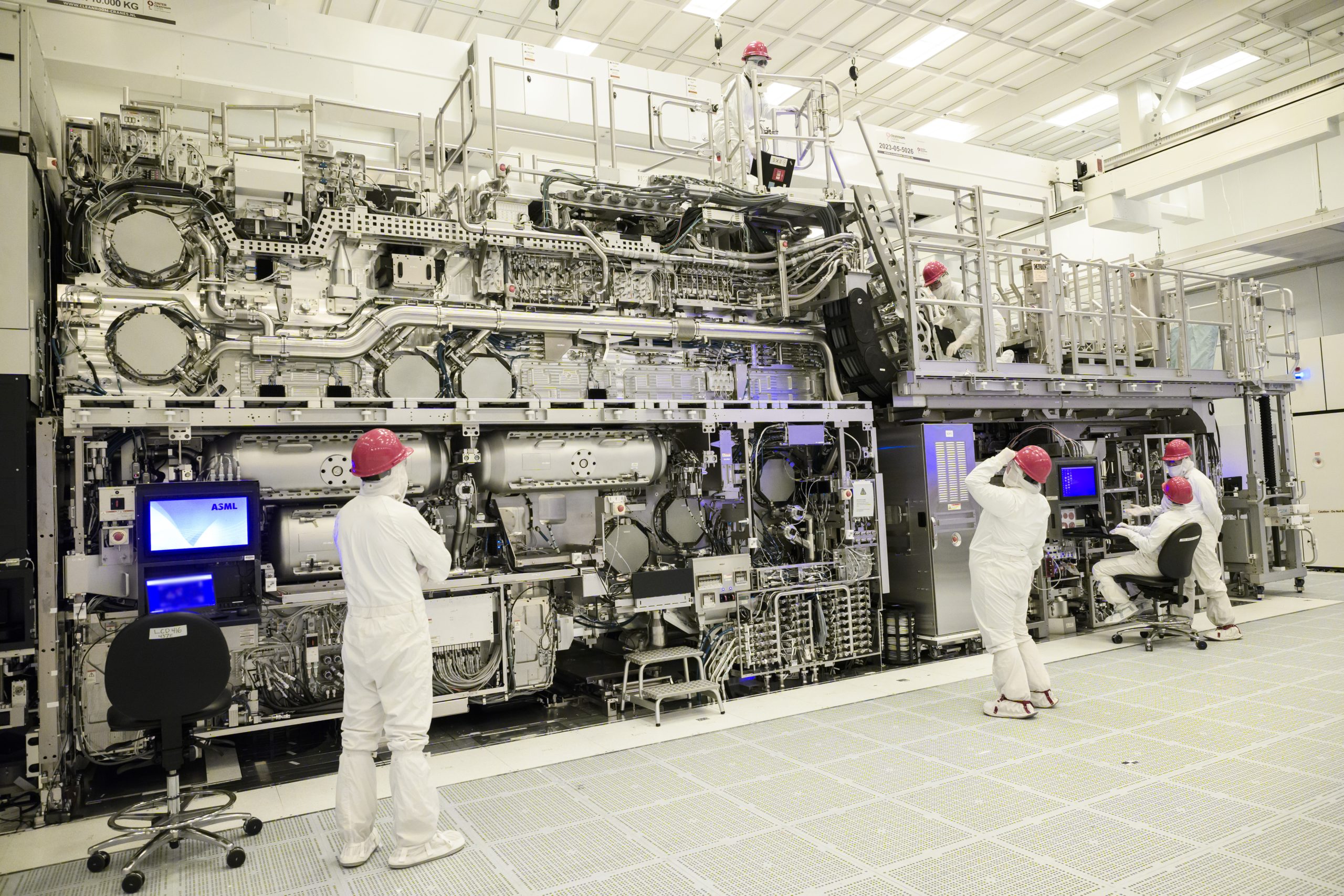
The method of applying and developing photoresist is another point of industry concern. Tokyo Electron currently dominates the standard wet process with spin-on coating and wet development in its track tools. Lam Research is attempting to gain share by promoting a dry deposition and dry development approach, done in its proprietary tools.
Conclusion
While Intel plans to adopt High-NA EUV for its 14A node, the company itself has stated that 14A is possible using only Low-NA EUV lithography (albeit, with multipatterning). That said, broad deployment may be deferred until the 1.0nm-class generation, when further cost reduction, process maturity, and infrastructure upgrades are more likely to align. For now, Intel’s early investments grant it an advantage in know-how, giving it a strategic edge as the technology matures.
Follow Tom’s Hardware on Google News to get our up-to-date news, analysis and reviews in your Google feeds. Make sure to click the Follow button.